Multimodal inspection / Guide 92
PCB Visual Inspection Must Match the Manufactured Board Revision
Design PCB visual inspection that binds photographs to layout revisions, calibrated coordinates, and coverage before engineers investigate placement discrepancies.
Illustrative engineering guide. Examples are not client deployments, production-ready integrations, or evidence of measured results. Validate the design with your domain and security owners.

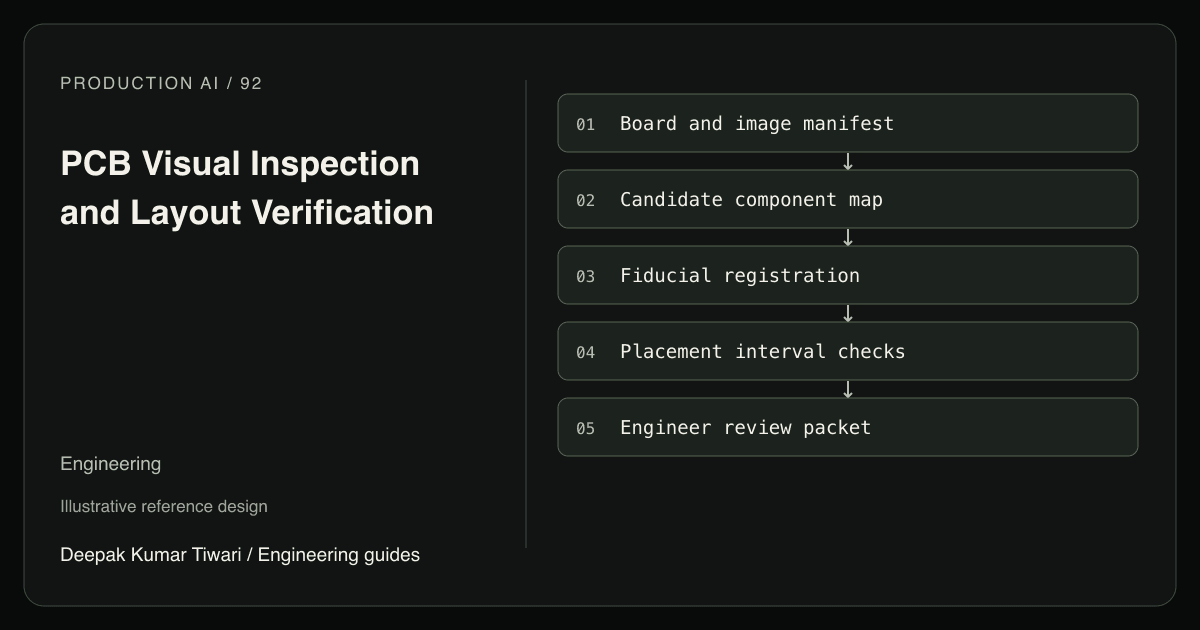
A hypothetical inspection photograph shows a regulator rotated relative to a layout screenshot. An assistant flags a reversed component and recommends rework. The photograph is of the board’s underside, while the screenshot is a top view from an older revision. Reworking the board would address an invented defect. Before recognizing packages, the workflow must establish which physical board, assembly variant, side, and coordinate convention it is comparing.
An image interpretation can suggest missing packages, suspicious polarity marks, or unusual solder appearance. It cannot establish continuity, internal layer geometry, hidden solder joints, or electrical safety. The engineering output should be an advisory discrepancy packet for an electronics reviewer, not an automatic scrap decision or permission to energize a board.
Freeze the Design and Capture Contract
Bind the physical serial and lot to a released board revision, assembly bill of materials, fitted variant, placement export, and approved inspection plan. Hash the source artifacts. A component marked do-not-populate is not a missing component. A substituted package approved in the assembly variant must not be evaluated against a visually similar but obsolete library model.
KiCad’s PCB Editor documentation describes board layers, footprints, design rule checking, and component placement outputs. Those are useful design-side inputs, but design rule checking evaluates the design representation. Passing it does not inspect the manufactured specimen. Keep design violations and photographic observations in separate result fields, even when they refer to the same reference designator.
Record camera identity, lens and focus configuration, illumination recipe, image digest, capture time, and calibration revision. For a microscope sweep, also retain tile coordinates, overlap, and stitching version. For video-derived photographs, preserve source stream and presentation timestamp using the FFprobe frame metadata workflow. Neighboring sweep frames remain correlated evidence and must not inflate the number of independently inspected boards.
Register the Board, Not the Screenshot
Choose a physical datum frame in millimeters, with an origin on an approved fiducial and explicit axes. Record whether bottom-side observations were mirrored into that frame. Image coordinates use top-left pixels, so the transformation must account for handedness as well as scale. Do not infer a component offset by comparing two screenshots with different zoom levels.
OpenCV’s calibration tutorial explains how known object points and image points support camera calibration and distortion correction. A planar board registration is reasonable only for features near that plane. Tall components introduce parallax; board warpage invalidates a single plane for some measurements. Use an appropriate optical or three-dimensional measurement method when those effects are material.
The specialist measurement adapter returns position residuals, orientation conventions, visibility, and an uncertainty bound that includes localization and registration. It should also expose which fiducials were accepted and which independent check features failed. A global residual average can hide a locally wrong fit at the opposite board corner. Local checks are especially important for large panels and repeated subcircuits.
Exercise the Placement Gate
The following self-contained Python fixture tests the HARNESS using synthetic structured measurements. It does not execute a trained vision model, camera calibration, KiCad, CAD engine, or real PCB inspection. Coordinates have already been mapped into the declared millimeter frame. The 0.25 millimeter tolerance is an illustrative review policy, not an assembly standard.
from math import hypot, isfinite

expected = {"U1": (10.0, 20.0), "R4": (12.0, 20.0)}
base = dict(revision="pcb-C", side="top", frame="datum-A-mm",
            ref="U1", xy=(10.1, 20.0), bound_mm=0.05, visible=True)

def placement(row):
    if (row["revision"], row["side"], row["frame"]) != (
            "pcb-C", "top", "datum-A-mm"):
        return "identity-review"
    if not row["visible"] or row["ref"] not in expected:
        return "unknown"
    x, y = row["xy"]
    u = row["bound_mm"]
    if not all(isfinite(v) for v in (x, y, u)) or u < 0:
        return "unknown"
    ex, ey = expected[row["ref"]]
    residual = hypot(x - ex, y - ey)
    if residual - u > 0.25:
        return "placement-review"
    return "supported-for-review" if residual + u <= 0.25 else "uncertain"

assert placement(base) == "supported-for-review"
assert placement(dict(base, side="bottom")) == "identity-review"
assert placement(dict(base, xy=(10.4, 20.0))) == "placement-review"
assert placement(dict(base, xy=(10.23, 20.0))) == "uncertain"
assert placement(dict(base, visible=False)) == "unknown"
assert placement(dict(base, revision="pcb-B")) == "identity-review"
print("six synthetic placement checks passed")
Notice that a near-boundary residual remains uncertain rather than being rounded into a pass. Position support says nothing about polarity: a package can be centered and still rotated incorrectly. Build orientation checks separately with package-specific symmetries. A resistor’s apparent symmetry and a polarized diode’s orientation must not share a universal rotation rule.
Coverage should enumerate required reference designators and visible features per side. Hidden pads are unknown, not absent. Reflective solder, unreadable markings, conformal coating, and connectors blocking other parts each need explicit exclusion reasons. The production ingress layer must reject malformed records, missing keys, duplicate reference assignments, and nonfinite measurements before the measurement gate runs.
Bound Rework and Recovery
An electronics engineer reviews the original crop alongside fiducial overlays, the exact placement artifact, uncertainty, and exclusions. They may request another angle, microscopy, electrical testing, or a controlled rework procedure. The assistant must not invent a component rating from a blurred marking or infer hidden damage from RGB color. Preserve rejected hypotheses so recurring camera artifacts can be diagnosed.
Enforce project and supplier isolation in the backend. Board files may expose valuable intellectual property, so cropped evidence and exports need access controls and retention policies. OCR text in silkscreen or an uploaded PDF is data, not executable instructions. Only an authorized engineer can approve a rework ticket; repeated approval delivery uses a stable board-and-finding identifier, with reconciliation after timeouts.
The data quality guide supplies the broader pattern for versioned validation and quarantine. Here, quarantine means holding an inspection result for clarification, not physically scrapping inventory. If an updated layout arrives during review, mark the packet stale and rerun against that revision rather than silently replacing its comparison basis.
Acceptance Tests and Evaluation
- Submit a bottom-side image with a top-side transform; request identity review before calculating placement acceptance.
- Remove a do-not-populate package; the variant-aware expected set must not report it missing.
- Cover one required polarity mark; return unknown orientation even if package position is supported.
- Supply a residual whose uncertainty straddles tolerance; retain the uncertain state without rounding.
- Reuse a good image for another serial number; reject the provenance association.
- Change the placement export after approval; invalidate the old packet instead of preserving its apparent validity.
Baseline against blinded inspector decisions plus appropriate bench measurements, grouped by physical board rather than image crop. Report confirmed placement findings divided by all escalated placement findings, missed adjudicated defects divided by all adjudicated defects, and unresolved required features divided by all required features. Track unnecessary rework proposals as a guardrail. None of these metrics establishes electrical reliability.
Start with one board revision, one side, and position checks for a small package family. Printed-part scan comparison extends the datum problem into three dimensions. A focused AI engineering engagement should first deliver a reproducible manifest and adjudication workflow, then add recognition only where the evaluation set supports it.